


India’s semiconductor journey has taken another big step forward. The Union Cabinet has approved Crystal Matrix’s project under the Compound Semiconductor Scheme of the India Semiconductor Mission (ISM).
The project will set up India’s first compound semiconductor GaN fab and ATMP (Assembly, Testing, Marking and Packaging) facility at Dholera Special Investment Region (SIR) in Gujarat.
This approval strengthens Dholera’s position as a leading semiconductor hub. It also marks India’s entry into the advanced world of Mini/Micro-LED display technology.
Project Overview: What the Dholera GaN Fab Brings
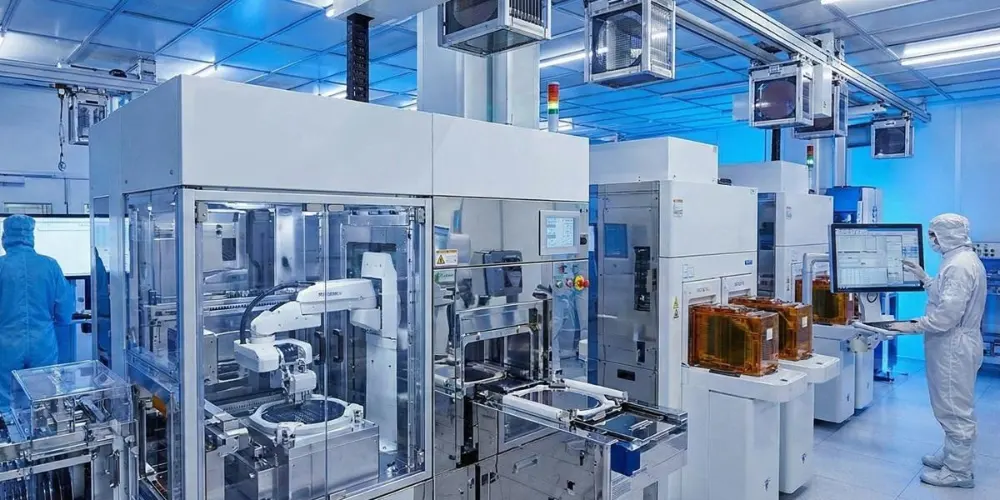
The Dholera GaN fab is backed by an investment of ₹3,068 crore. It will be built on 40 acres of land within Dholera SIR.
The facility will focus on two core products:
- Mini/Micro-LED display panels
- GaN (Gallium Nitride) epitaxy wafers
Together, these products will help India build capabilities in compound semiconductors and next-generation display technologies. Until now, India has depended largely on imports for both.
Production Capacity and Key Numbers
The planned capacity of the facility is significant for a first-of-its-kind project in India.
| Parameter | Details |
| Investment | ₹3,068 crore |
| Area Allotted | 40 acres in Dholera SIR |
| RGB GaN Wafers | 24,000 sets (each) per year |
| Mini/Micro-LED Display Panels | 72,000 sq. m per year |
| Direct Jobs | 1,600+ |
The annual output of 24,000 sets each of RGB GaN wafers will cover red, green and blue components. These are the building blocks of full-colour Micro-LED displays.
The 72,000 square metres of display panels per year will feed demand from consumer electronics, automotive and commercial display markets.
Why GaN and Micro-LED Technology Matter
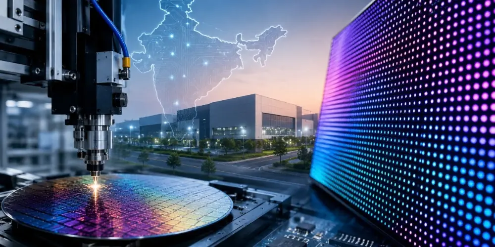
Gallium Nitride is a compound semiconductor. Unlike traditional silicon, it offers higher efficiency, better heat handling and superior light emission.
GaN is widely used in LEDs, fast chargers, power electronics, 5G equipment and electric vehicles. It is one of the most strategic materials in modern electronics.
Micro-LED is often called the future of display technology. It offers:
- Higher brightness than OLED
- Better energy efficiency
- Longer lifespan with no burn-in
- Deeper contrast and sharper colours
Mini-LED, its close cousin, is already used in premium TVs, laptops and monitors. By producing both at home, India can reduce import dependence and join a high-value global supply chain.
Understanding the ATMP Component
ATMP stands for Assembly, Testing, Marking and Packaging. It is the stage where fabricated chips and wafers are turned into usable products.
Having both a fab and an ATMP unit at the same site is a major advantage. It shortens the supply chain, cuts logistics costs and speeds up delivery.
This integrated model also makes the Dholera facility more attractive to global customers looking for reliable, end-to-end manufacturing partners.
Why Dholera Is Becoming India’s Semiconductor Hub
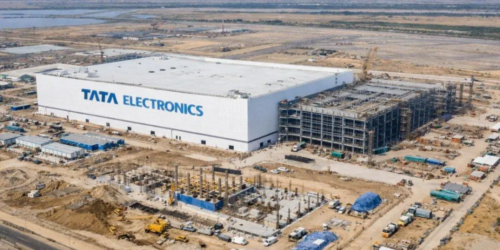
Dholera SIR in Gujarat is India’s first greenfield smart industrial city. It has been planned with large land parcels, reliable power, water supply and modern infrastructure.
These features are essential for semiconductor manufacturing, which needs uninterrupted utilities and ultra-clean environments.
Dholera already hosts India’s first commercial semiconductor fab being built by Tata Electronics. The addition of the Crystal Matrix GaN project builds a cluster effect. Suppliers, talent and support industries tend to follow such clusters.
Strong state policy support from Gujarat and central incentives under ISM further boost investor confidence in the region.
Job Creation and Skill Development
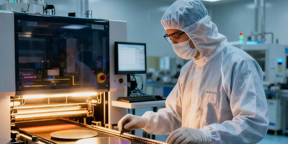
The project is expected to generate more than 1,600 direct jobs. Many more indirect jobs are likely in logistics, construction, services and supply chains.
These roles will require engineers, technicians, material scientists and quality specialists. This will help build a skilled workforce trained in advanced compound semiconductor processes.
Over time, this talent pool will become a key asset for India. It will support future investments and help the country move up the technology value chain.
Boost to Atmanirbhar Bharat and Global Supply Chains
The Dholera GaN fab fits directly into India’s vision of a resilient and self-reliant semiconductor ecosystem.
Global supply chains for chips and displays are concentrated in a few countries. Disruptions in recent years showed how risky this can be.
By building domestic capacity in GaN wafers and Micro-LED panels, India gains:
- Lower import dependence in a strategic sector
- A stronger position in global electronics supply chains
- Support for local electronics, EV and defence manufacturing
- Higher-value exports in the long term
The project also complements the Production Linked Incentive (PLI) schemes for electronics and IT hardware.
Conclusion
The approval of Crystal Matrix’s ₹3,068 crore project is a milestone for Indian manufacturing. The Dholera GaN fab will be India’s first compound semiconductor facility of its kind, focused on Mini/Micro-LED displays and GaN epitaxy wafers.
With 40 acres of land, strong production capacity and over 1,600 direct jobs, the project adds real depth to India’s semiconductor mission. It also confirms Dholera’s rise as the country’s leading semiconductor destination.
As more fabs, ATMP units and suppliers arrive, Dholera is set to become the heart of India’s chip-making future.